Designing Printed Circuit Boards (PCBs) is a critical stage in the development of electronic devices, serving as the foundation for their functionality and performance. From concept to production, every aspect of PCB design demands careful consideration to ensure optimal functionality, reliability, and manufacturability. In this guide, we’ll delve into the intricacies of PCB design and explore essential principles and best practices to help you navigate this complex process successfully.
Understanding the Basics: Before diving into PCB design, it’s crucial to grasp the fundamentals of electronic circuitry and component placement. Familiarize yourself with key components such as resistors, capacitors, diodes, and integrated circuits, and learn how they interact within the circuit.
Choosing the Right Software: Selecting the appropriate PCB design software is paramount to streamline the design process and achieve accurate results. Popular tools like Altium Designer, Eagle PCB, and KiCad offer robust features for schematic capture, component placement, routing, and simulation, catering to the diverse needs of designers and engineers.
Schematic Design: The schematic serves as the blueprint for your PCB design, illustrating the interconnections between components and their respective functions. Pay meticulous attention to detail during schematic creation, ensuring clarity, organization, and adherence to design specifications.
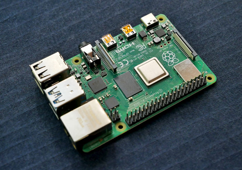
Component Placement: Efficient component placement is essential for optimizing signal integrity, minimizing interference, and facilitating ease of assembly. Consider factors such as component density, signal flow, thermal management, and accessibility when arranging components on the PCB layout.
Routing: Routing entails the creation of electrical pathways (traces) that connect components and facilitate the flow of signals throughout the circuit. Employ strategic routing techniques to minimize signal distortion, avoid signal crosstalk, and optimize signal integrity. Pay close attention to trace width, impedance matching, and signal integrity guidelines to mitigate potential issues.
Grounding and Power Distribution: Establishing robust grounding and power distribution schemes is critical to ensure stable operation and minimize electromagnetic interference (EMI). Implement separate ground planes for analog and digital circuits, employ bypass capacitors for noise suppression, and optimize power delivery networks to maintain voltage stability and reduce power losses.
Design Rule Checking (DRC) and Validation: Conduct thorough design rule checking (DRC) and validation to identify and rectify potential errors, inconsistencies, and manufacturability issues early in the design process. Utilize design rule checkers and simulation tools to verify design compliance with industry standards, manufacturability constraints, and performance specifications.
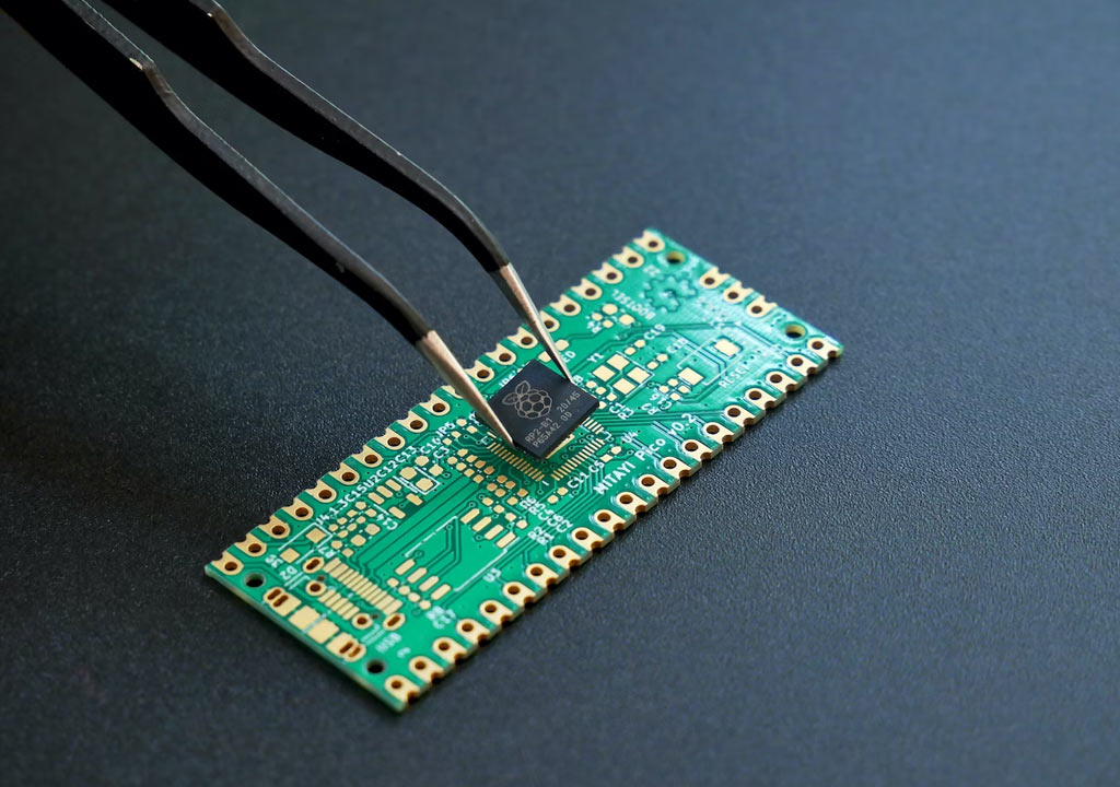
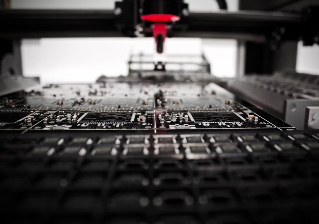
Prototyping and Testing: Prototyping and testing are indispensable phases in the PCB design cycle, allowing designers to evaluate the functionality, performance, and reliability of their designs in real-world scenarios. Fabricate prototype boards using reliable PCB manufacturing services and conduct comprehensive testing to validate design integrity and identify areas for improvement.
Designing Printed Circuit Boards is a multifaceted endeavor that requires a blend of technical expertise, creativity, and attention to detail. By adhering to best practices, leveraging advanced design tools, and embracing iterative design methodologies, designers can craft PCBs that meet the highest standards of performance, reliability, and manufacturability. With a solid foundation in PCB design principles and a commitment to continuous learning and improvement, designers can unlock endless possibilities in the realm of electronics innovation.